- 您现在的位置:买卖IC网 > Sheet目录3871 > PIC16F72-I/ML (Microchip Technology)IC PIC MCU FLASH 2KX14 28-QFN
PIC16F72
DS39597C-page 10
2007 Microchip Technology Inc.
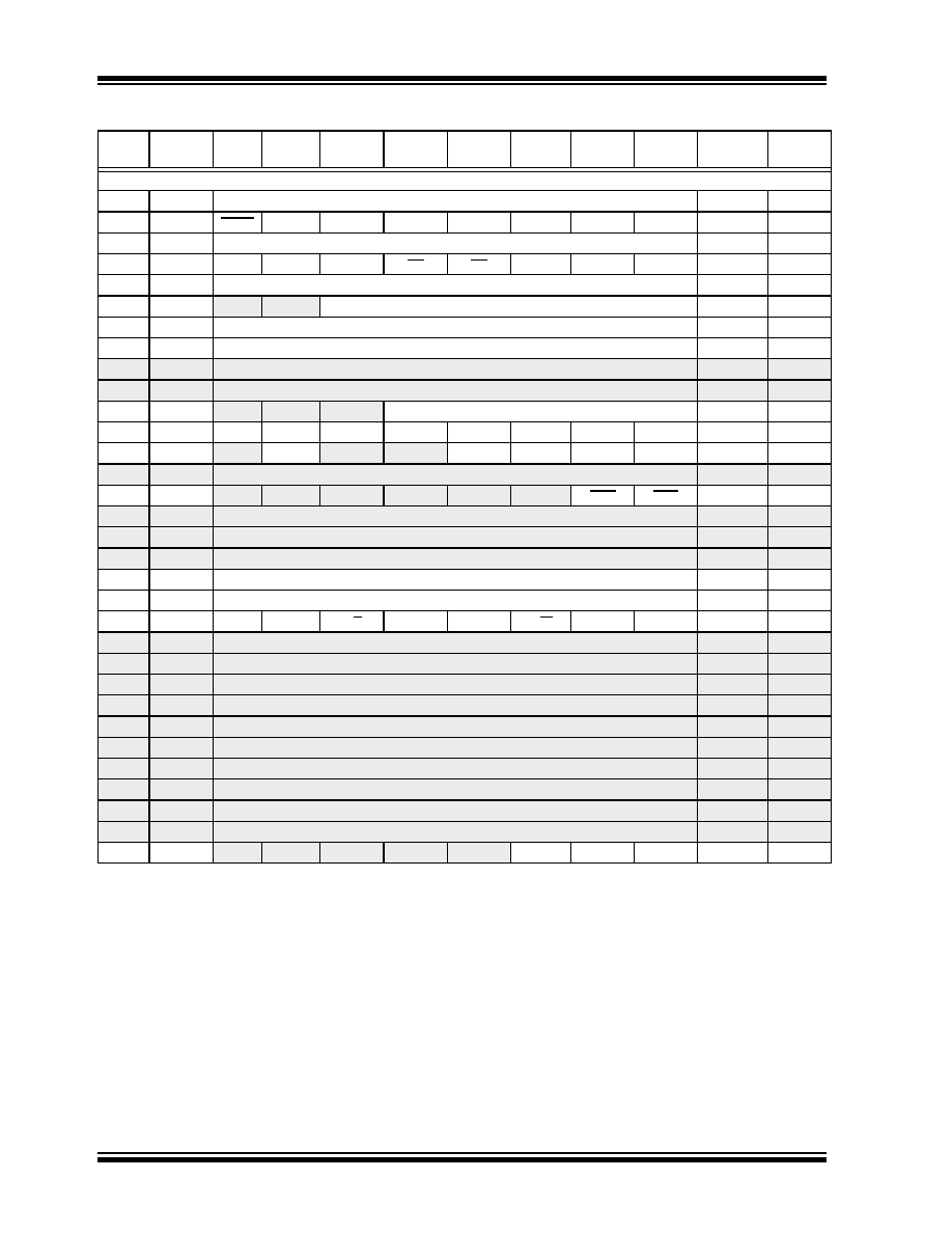
Bank 1
80h(1)
INDF
Addressing this location uses contents of FSR to address data memory (not a physical register) 0000 0000
81h
OPTION
RBPU
INTEDG
T0CS
T0SE
PSA
PS2
PS1
PS0
1111 1111
82h(1)
PCL
Program Counter's (PC) Least Significant Byte
0000 0000
83h(1)
STATUS
IRP
RP1
RP0
TO
PD
ZDC
C
0001 1xxx
84h(1)
FSR
Indirect Data Memory Address Pointer
xxxx xxxx
85h
TRISA
—
PORTA Data Direction Register
--11 1111
86h
TRISB
PORTB Data Direction Register
1111 1111
87h
TRISC
PORTC Data Direction Register
1111 1111
88h
—
Unimplemented
—
89h
—
Unimplemented
—
8Ah(1,2)
PCLATH
—
Write Buffer for the upper 5 bits of the PC
---0 0000
8Bh(1)
INTCON
GIE
PEIE
TMR0IE
INTE
RBIE
TMR0IF
INTF
RBIF
0000 000x
8Ch
PIE1
—ADIE
—
SSPIE
CCP1IE
TMR2IE
TMR1IE
-0-- 0000
8Dh
—
Unimplemented
—
8Eh
PCON
—
—POR
BOR
---- --qq
8Fh
—
Unimplemented
—
90h
—
Unimplemented
—
91h
—
Unimplemented
—
92h
PR2
Timer2 Period Register
1111 1111
93h
SSPADD
Synchronous Serial Port (I2C mode) Address Register
0000 0000
94h
SSPSTAT
SMP
CKE
D/A
PS
R/W
UA
BF
0000 0000
95h
—
Unimplemented
—
96h
—
Unimplemented
—
97h
—
Unimplemented
—
98h
—
Unimplemented
—
99h
—
Unimplemented
—
9Ah
—
Unimplemented
—
9Bh
—
Unimplemented
—
9Ch
—
Unimplemented
—
9Dh
—
Unimplemented
—
9Eh
—
Unimplemented
—
9Fh
ADCON1
—
PCFG2
PCFG1
PCFG0
---- -000
TABLE 2-1:
SPECIAL FUNCTION REGISTER SUMMARY (CONTINUED)
Address
Name
Bit 7
Bit 6
Bit 5
Bit 4
Bit 3
Bit 2
Bit 1
Bit 0
Value on
POR, BOR
Details on
page:
Legend:
x
= unknown, u = unchanged, q = value depends on condition, - = unimplemented, read as ‘0’, r = reserved.
Shaded locations are unimplemented, read as ‘0’.
Note
1:
These registers can be addressed from any bank.
2:
The upper byte of the program counter is not directly accessible. PCLATH is a holding register for the PC<12:8> whose
contents are transferred to the upper byte of the program counter.
3:
This bit always reads as a ‘1’.
发布紧急采购,3分钟左右您将得到回复。
相关PDF资料
XF2R34154A
CONN FPC 34POS 0.5MM PITCH SMD
XF2R24154A
CONN FPC 24POS 0.5MM PITCH SMD
PIC18F45K20-I/ML
IC PIC MCU FLASH 16KX16 44QFN
PIC18F14K50-I/SO
IC PIC MCU FLASH 8KX16 20-SOIC
PIC16F628A-I/SS
IC MCU FLASH 2KX14 EEPROM 20SSOP
PIC18LF43K22-I/PT
IC PIC MCU 8KB FLASH 44TQFP
DSPIC33FJ16MC101-I/SO
IC DSP 16BIT 16KB 20SOIC
PIC12C672-04I/SM
IC MCU OTP 2KX14 A/D 8-SOIJ
相关代理商/技术参数
PIC16F72-I/MLG
功能描述:8位微控制器 -MCU 3.5KB 128 RAM 22 I/O Lead Free Package RoHS:否 制造商:Silicon Labs 核心:8051 处理器系列:C8051F39x 数据总线宽度:8 bit 最大时钟频率:50 MHz 程序存储器大小:16 KB 数据 RAM 大小:1 KB 片上 ADC:Yes 工作电源电压:1.8 V to 3.6 V 工作温度范围:- 40 C to + 105 C 封装 / 箱体:QFN-20 安装风格:SMD/SMT
PIC16F72-I/SO
功能描述:8位微控制器 -MCU 3.5KB 128 RAM 22 I/O
RoHS:否 制造商:Silicon Labs 核心:8051 处理器系列:C8051F39x 数据总线宽度:8 bit 最大时钟频率:50 MHz 程序存储器大小:16 KB 数据 RAM 大小:1 KB 片上 ADC:Yes 工作电源电压:1.8 V to 3.6 V 工作温度范围:- 40 C to + 105 C 封装 / 箱体:QFN-20 安装风格:SMD/SMT
PIC16F72-I/SO
制造商:Microchip Technology Inc 功能描述:8BIT FLASH MCU SMD 16F72 SOIC28
PIC16F72-I/SOG
功能描述:8位微控制器 -MCU 3.5KB 128 RAM 22 I/O Lead Free Package RoHS:否 制造商:Silicon Labs 核心:8051 处理器系列:C8051F39x 数据总线宽度:8 bit 最大时钟频率:50 MHz 程序存储器大小:16 KB 数据 RAM 大小:1 KB 片上 ADC:Yes 工作电源电压:1.8 V to 3.6 V 工作温度范围:- 40 C to + 105 C 封装 / 箱体:QFN-20 安装风格:SMD/SMT
PIC16F72-I/SP
功能描述:8位微控制器 -MCU 3.5KB 128 RAM 22 I/O
RoHS:否 制造商:Silicon Labs 核心:8051 处理器系列:C8051F39x 数据总线宽度:8 bit 最大时钟频率:50 MHz 程序存储器大小:16 KB 数据 RAM 大小:1 KB 片上 ADC:Yes 工作电源电压:1.8 V to 3.6 V 工作温度范围:- 40 C to + 105 C 封装 / 箱体:QFN-20 安装风格:SMD/SMT
PIC16F72-I/SP
制造商:Microchip Technology Inc 功能描述:IC 8BIT FLASH MCU 16F72 SDIL28
PIC16F72-I/SS
功能描述:8位微控制器 -MCU 3.5KB 128 RAM 22 I/O
RoHS:否 制造商:Silicon Labs 核心:8051 处理器系列:C8051F39x 数据总线宽度:8 bit 最大时钟频率:50 MHz 程序存储器大小:16 KB 数据 RAM 大小:1 KB 片上 ADC:Yes 工作电源电压:1.8 V to 3.6 V 工作温度范围:- 40 C to + 105 C 封装 / 箱体:QFN-20 安装风格:SMD/SMT
PIC16F72-I/SS
制造商:Microchip Technology Inc 功能描述:8BIT FLASH MCU SMD 16F72 SSOP28